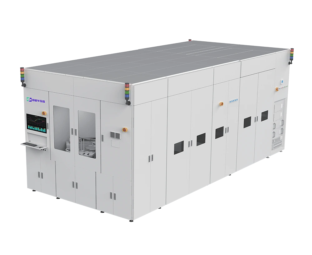
This product is a vertical hot-wall CVD epitaxial system designed specifically for 6/8-inch silicon carbide power devices and compound semiconductors. Featuring vertical gas injection and a high-speed rotating susceptor, the system delivers excellent film thickness and doping uniformity, a high growth rate, and low defect density. It mainly consists of a vertical hot-wall reaction chamber, a high-vacuum transfer system, a laminar-flow gas distribution system, a high-temperature exhaust gas treatment system, and a high-precision temperature control system. It is an ideal mass-production platform for preparing epitaxial layers for SiC high-voltage devices.
This product is a vertical hot-wall CVD epitaxial system designed specifically for 6/8-inch silicon carbide power devices and compound semiconductors. Featuring vertical gas injection and a high-speed rotating susceptor, the system delivers excellent film thickness and doping uniformity, a high growth rate, and low defect density. It mainly consists of a vertical hot-wall reaction chamber, a high-vacuum transfer system, a laminar-flow gas distribution system, a high-temperature exhaust gas treatment system, and a high-precision temperature control system. It is an ideal mass-production platform for preparing epitaxial layers for SiC high-voltage devices.
Vertical laminar-flow gas injection combined with a high-speed rotating susceptor ensures uniform flow and thermal fields across the wafer surface. Film thickness uniformity is ≤1.5%, and doping concentration uniformity is ≤1.5%. It also effectively suppresses fatal defects such as triangular defects and fall-on particles.
High-Throughput Design
Supports simultaneous epitaxy of multiple 6/8-inch wafers. With optimized flow and thermal fields in the reaction chamber, it achieves a high growth rate of over 50 μm/h, meeting the mass-production requirements for thick-film epitaxy of SBDs and MOSFETs.
In-situ Etching and Multi-Process Integration
Integrated in-situ HCl/H₂ cleaning and chamber etching functions significantly reduce particles, extend equipment maintenance cycles, and support uninterrupted continuous growth of buffer/drift layers.
High Maintainability
The open-close furnace body and modular susceptor design allow rapid replacement of reactor internals and graphite thermal field components, significantly shortening PM and equipment restart time and reducing long-term cost of ownership.
High-Precision Temperature Control
Equipped with multi-zone heating and a multi-wavelength optical pyrometry system, it enables real-time precise control and adjustment of the epitaxial growth temperature, ensuring precise repeatability of high-purity semi-insulating and n/p-type doping processes.
Applicable Fields
Compound Semiconductor Power Devices (SiC MOSFET/SBD, etc.)